Building a quantum processor feels like trying to assemble a Swiss watch inside a hurricane. You need extreme precision, zero dust, and temperatures colder than deep space. If you want to learn these advanced hardware skills, check out the comprehensive training at QuantumOpsSchool.com to master the exact tools used by top engineers.
Standard computer chips use billions of tiny switches called transistors. Quantum chips use qubits instead. These qubits can hold multiple states at once thanks to weird laws of physics. But building them is tough. A single stray atom or tiny scratch on the surface can ruin the whole device.
That is why scientists and engineers use high-tech cleanrooms. These rooms have air filters that trap almost every speck of dust. Workers wear full-body suits to keep skin flakes and hair away from the delicate silicon wafers.
In this guide, you will learn how engineers build these amazing chips from start to finish. We will look at the materials, the machines, and the step-by-step methods used in modern labs. Let us jump right into the core concepts.
Understanding the Foundation: Silicon Wafers and Substrates
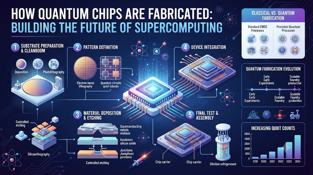
Every quantum chip starts with a pure silicon or sapphire disk called a wafer. Think of this wafer as the blank canvas for your microscopic circuit.
Before any building begins, the wafer must be spotless. Workers wash the disk in chemical baths to strip away oils and dust. Any leftover dirt will block the tiny patterns we need to print later.
Once clean, the wafer goes into a vacuum chamber. Here, a thin metal film is sprayed across the top surface. This metal is usually aluminum or niobium because they become superconducting at ultra-low temperatures.
Etching Circuits with Light
How do you carve lines that are thousands of times thinner than a human hair? You use a trick called photolithography.
First, workers coat the metal film in a special chemical called a photoresist. This chemical changes when light hits it. Next, a machine shines ultraviolet light through a stencil template onto the wafer.
The exposed parts of the chemical wash away in a liquid bath. Then, a strong chemical spray eats away the bare metal underneath. What remains is a precise network of wires and qubit pads.
The Role of Cryogenics in Testing
You cannot test a quantum chip at room temperature. Heat causes random vibrations that destroy fragile quantum states.
Instead, engineers mount the finished chip onto a special gold-plated copper plate. They place this plate inside a massive machine called a dilution refrigerator.
This fridge cools the chip down to just a fraction of a degree above absolute zero. At this temperature, the metal wires lose all electrical resistance and allow qubits to talk to each other.
Real-World Story About Server Crashes / Case Studies
- A major quantum lab suffered total wafer contamination because a technician wore the wrong grade of gloves inside the cleanroom, ruining a week of work.
- A research team faced severe signal interference until they redesigned the ground planes on their chip to block stray radio waves.
- An experimental setup kept losing qubit coherence because a tiny air leak in the dilution fridge let room-temperature heat creep inside.
- A manufacturing crew noticed widespread etching flaws caused by an old ultraviolet lamp losing its light intensity over time.
- A university team accidentally ruined an entire batch of qubits by using a chemical cleaner that was slightly past its expiration date.
- A quantum startup solved persistent wiring shorts by switching to a cleaner vacuum deposition machine with better particle control.
- An engineering group fixed sudden chip drops during cooling by changing the thermal paste used to mount the sample holder.
- A national lab overcame low qubit yields by upgrading their optical alignment tools to achieve nanometer-level precision.
- A development team stopped mysterious data spikes by shielding their control electronics inside a heavy copper box.
- A commercial vendor improved chip lifespan by baking the silicon wafers longer to drive out trapped moisture before metal deposition.
Comparing Quantum vs. Classical Chip Fabrication
| Feature | Classical Silicon Chips | Quantum Superconducting Chips |
| Primary Unit | Transistor | Qubit |
| Operating Temp | Room Temperature | Absolute Zero ($0.01\text{ K}$) |
| Material Base | Pure Silicon | Silicon, Sapphire, Aluminum |
| Error Rate | Extremely Low | High (Needs Error Correction) |
| Cleanroom Need | Standard High-Tech | Ultra-Clean Nanofabrication |
Common Mistakes and Pitfalls
- Skipping wafer cleaning steps: Leaving microscopic grease spots on the disk ruins the metal bond. Always follow a strict multi-stage chemical wash.
- Ignoring thermal expansion: Different materials expand at different rates when cooled. Match your substrate and metal layers carefully to avoid cracks.
- Using low-purity gases: Impure reactive gases leave chemical residue inside the etching chamber. Buy certified ultra-pure lab supplies.
- Rushing the vacuum pump-down: Trapped air bubbles in the chamber cause uneven film thickness. Wait for full vacuum pressure before deposition.
- Neglecting electrostatic discharge: A tiny static shock from your hand can fry a sensitive qubit. Always wear grounded wrist straps.
- Overheating during wire bonding: Too much heat melts the delicate superconducting pads. Use low-power ultrasonic bonders.
- Failing to calibrate lasers: An uncalibrated photolithography laser carves lines that are too thick or too thin. Test your light source daily.
- Ignoring ambient magnetic fields: Earth’s magnetic field can scramble qubits. Install mu-metal shields around your test cryostat.
- Skipping intermediate testing: Waiting until the very end to test the chip makes it hard to find faults. Test individual components early.
- Poor documentation: Forgetting which chemical batch was used makes troubleshooting impossible. Keep a detailed digital lab notebook.
Step-by-Step Implementation Roadmap
- Step 1: Wafer Preparation: Clean a high-purity silicon or sapphire disk using acid baths and deionized water rinses.
- Step 2: Substrate Insulation: Grow a thin layer of silicon dioxide on top of the wafer to isolate the electrical circuits.
- Step 3: Thin Film Deposition: Place the wafer inside a vacuum chamber and coat it with a uniform layer of superconducting aluminum.
- Step 4: Photoresist Coating: Spin a liquid light-sensitive polymer across the metal surface at high speed to form a smooth film.
- Step 5: Optical Lithography: Shine ultraviolet light through a precise mask pattern to expose the design onto the photoresist.
- Step 6: Chemical Development: Wash the wafer in a developer solution to dissolve the exposed photoresist and reveal the pattern.
- Step 7: Plasma Etching: Use reactive ion etching to eat away the exposed metal, leaving behind the final qubit circuits.
- Step 8: Residue Stripping: Remove the remaining photoresist layer using safe solvents and oxygen plasma cleaning.
- Step 9: Packaging and Dicing: Cut the large wafer into individual quantum chips and attach them to gold carrier boards.
- Step 10: Cryogenic Testing: Mount the finished chip inside a dilution refrigerator and run initial microwave resonance tests.
Frequently Asked Questions
1. What materials are used to make quantum chips?
Most superconducting quantum chips use a silicon or sapphire base coated with thin layers of aluminum, niobium, or tantalum.
2. Why do quantum chips need ultra-cold temperatures?
Heat causes thermal vibrations that disrupt fragile quantum states. Cooling keeps the qubits stable and reduces electrical noise.
3. How small are the features on a quantum processor?
Features like Josephson junctions are often measured in nanometers, making them thousands of times thinner than a human hair.
4. Can standard computer factories make quantum chips?
Some steps use standard silicon tools, but quantum chips require specialized ultra-clean rooms and precise superconducting materials.
5. What is a qubit?
A qubit is the basic unit of quantum information, capable of existing in multiple states at the same time.
6. How do engineers test quantum chips?
Engineers use microwave pulses to control the qubits and measure their response inside a dilution refrigerator.
7. Why is dust such a big problem in fabrication?
A single speck of dust can bridge two microscopic wires and cause an instant short circuit on the chip.
8. What is photolithography?
Photolithography is a process that uses light and stencils to print micro-scale circuit patterns onto a silicon wafer.
9. How long does it take to make a quantum chip?
Fabricating a batch of wafers usually takes several days, followed by days of cooling and testing in a lab.
10. Where can I learn more about quantum hardware?
You can explore deep training resources and guides by visiting QuantumOpsSchool.com.
Final Recommendation and Next Steps
Building quantum chips requires patience, precision, and strict adherence to cleanroom protocols. Start small by studying basic semiconductor physics before moving on to multi-qubit processor designs. Keep your workspace clean, test your equipment frequently, and always double-check your calibration settings.